Welcome: Supsemi Electronic Technology Co., Ltd

sales@supsemi.com
+86-18059149998
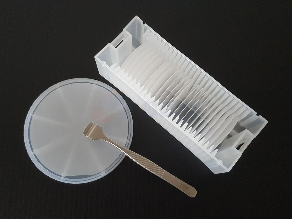
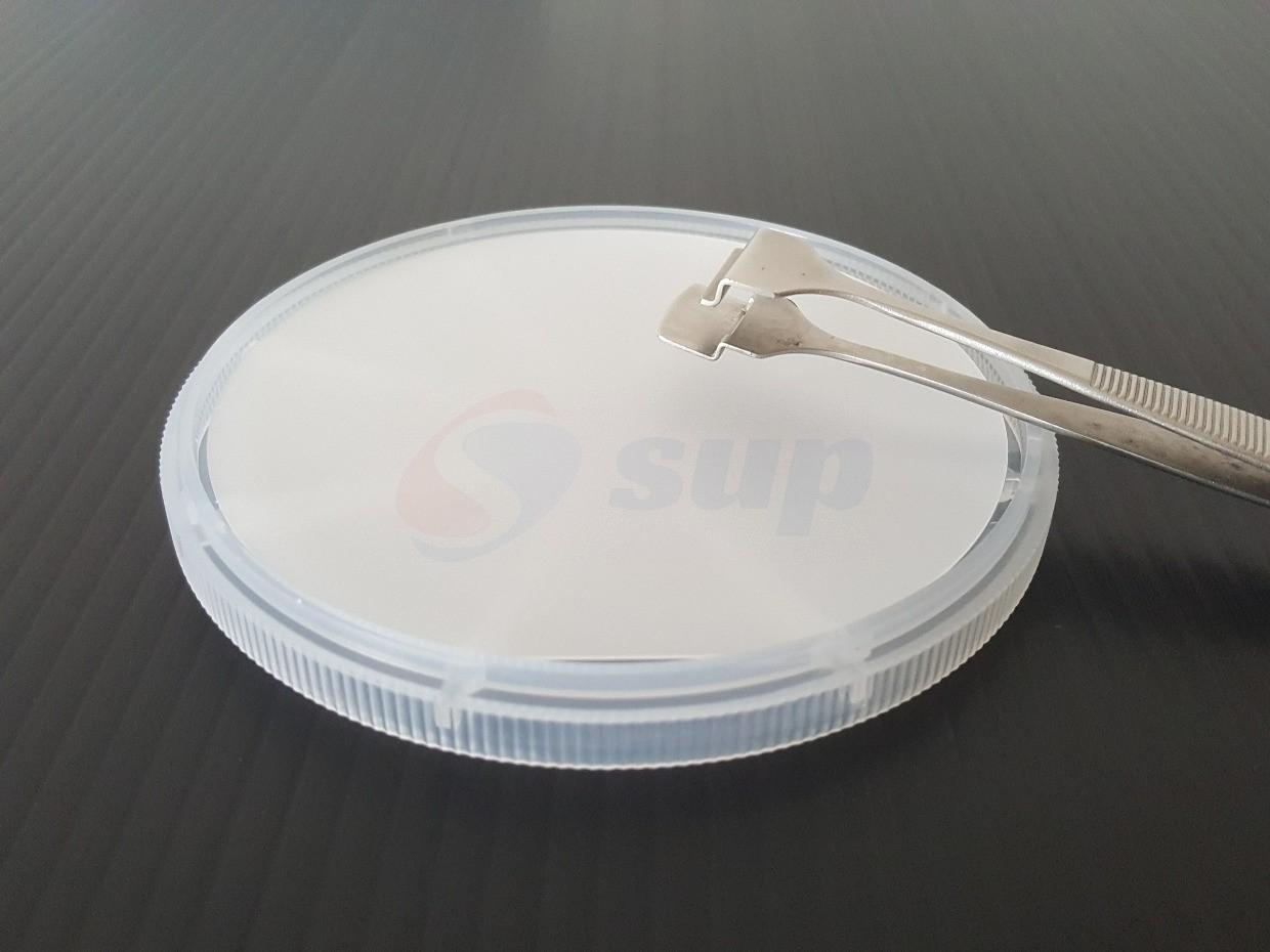
Product Name: Sapphire Wafers
Product Material: 99.996% of Al203,High Purity, Monocrystalline, Al203
Orientation: C-plane (0001)to M-plane(1-100)or A-plane(1 1-2 0)0.2±0.1°10.3+0,1°,R-plane(1-102),A-plane(1 1-2 0),M-plane(1-1 0 0),AnyOrientation ,Any angle
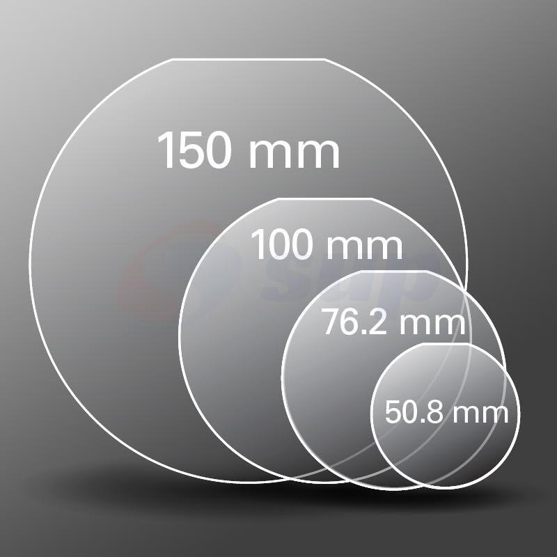
Product Sizes: 2 inches/4 inches/6 inches/8 inches (Customizable)
Diameter: 2-3-4-6-inch
Customization with Drawings is Welcome.
# Sapphire Wafers for Semiconductor & Materials Research: Precision You Can Trust
For researchers in semiconductor and materials labs worldwide, the quality of your substrate directly impacts the reliability of your data. Our research-grade sapphire wafers are engineered to solve the unique challenges of academic and industrial R&D—whether you're growing GaN epitaxial layers, testing optoelectronic device performance, or exploring next-gen semiconductor materials.

## Why Our Sapphire Wafers Stand Out for Your Lab?
### 1. Tailored to Research Needs: Small Batches, Big Consistency
We understand lab work thrives on flexibility. Unlike mass-production suppliers, we specialize in small-batch orders (starting from 1 piece) with the same precision as industrial-scale products. This means:
- No minimum order constraints: Test new hypotheses without overcommitting to large quantities.
- Consistent quality across runs: Every wafer undergoes strict inspection (surface roughness <0.5 nm RMS, thickness tolerance ±5 μm) to ensure your experiments are repeatable—critical for publishing reliable results.
- Customizable specs: Choose from 2”, 4”, or 6” diameters, with options for c-plane, m-plane, or r-plane orientations to match your epitaxial growth requirements (e.g., GaN on c-plane sapphire for LED research).

### 2. Built for the Harshest Lab Environments
Sapphire's inherent properties—extreme temperature resistance (up to 2050°C), chemical inertness, and low defect density—make it ideal for demanding experiments. Our wafers enhance these advantages:
- Withstand aggressive processes: Perfect for MOCVD, MBE, or wet etching studies involving HF, plasma, or high-temperature annealing.
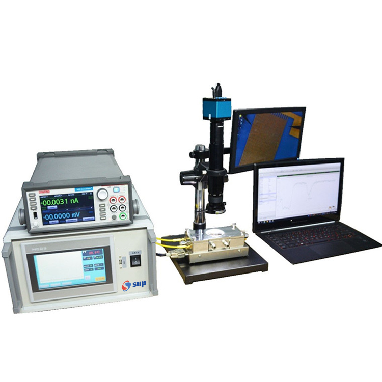
- Minimize experimental noise: Ultra-clean surfaces (particle count <10 particles/ft² for sizes >0.5 μm) reduce contamination risks in sensitive tests, such as thin-film growth characterization via AFM or XRD.
- Compatible with diverse setups: Works seamlessly with lab-scale deposition tools, Probe Stations, and vacuum chambers—no need to modify your equipment.

### 3. More Than a Substrate: A Partner in Your Research
We don’t just supply wafers—we support your goals:
- Technical insights: Our team includes materials scientists with expertise in semiconductor research. Need help selecting the right orientation for your AlN growth project? We'll guide you.
- Fast turnaround: Get small batches in 1-2 weeks, so you can keep pace with tight research timelines (e.g., meeting conference abstract deadlines).
- Cost-effective for labs: Competitive pricing on small quantities, with discounts for academic institutions—designed to fit research grant budgets.
Whether you’re developing next-gen power devices, optimizing UV detector performance, or exploring novel wide-bandgap semiconductors, our sapphire wafers deliver the precision and reliability your research demands.
Ready to discuss your specific needs? Contact us for a free sample quote or technical datasheet.
Office Photo

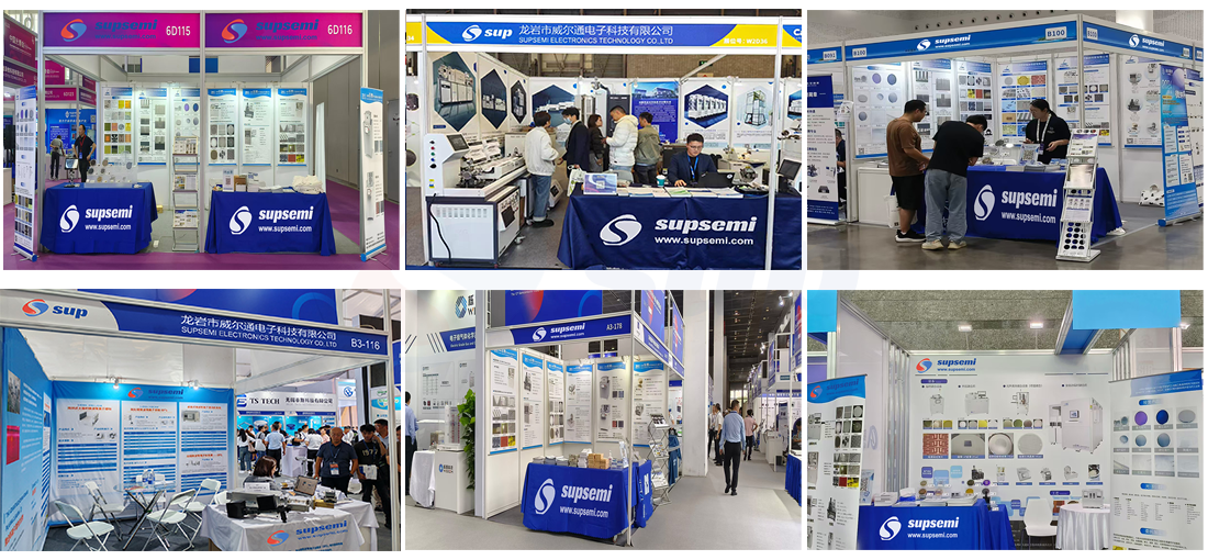
Exhibition
Contact: Bruce Liu
WhatsApp: +86-18059149998
Tel: +86-18059149998
Email: sales@supsemi.com
Add: Room 1402, Building 1, No. 89 Xibeilu, Xishancun, Xibei Street, Xinluo District, Longyan City, Fujian Province
We chat