Welcome: Supsemi Electronic Technology Co., Ltd

sales@supsemi.com
+86-18059149998
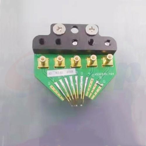
Wafer probe card is a key interface component in wafer-level testing during semiconductor manufacturing. It connects chips to test systems via probes contacting pads or bumps, transmitting signals to detect electrical performance and screen out defects before dicing and packaging.
Supsemi is a professional probe card manufacturer, capable of designing, processing, and custom-producing the probe cards you need.
Supsemi is a professional probe card manufacturer, capable of designing, processing, and custom-producing the probe cards you need.
[Request Technical Datasheet →] | [Discuss Custom Configuration →]
Wafer Probe Cards: Engineering Precision for Semiconductor Research
For researchers engaged in semiconductor material characterization, device prototyping, and process validation, the reliability of wafer-level testing hinges on probe card performance. Our wafer probe cards are engineered with research-specific technical specifications to address the complexities of academic lab environments—from low-volume, high-variability samples to cutting-edge material systems.
Technical Specifications for Research Applications
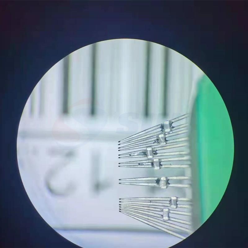
Probe Tip Engineering: Available in tungsten, palladium-alloy, and diamond-coated variants, with tip radii ranging from 1μm to 50μm. This allows precise contact with diverse pad materials (Al, Cu, Au, and emerging 2D material interfaces) while minimizing contact resistance (<50mΩ typical) and preventing pad delamination.

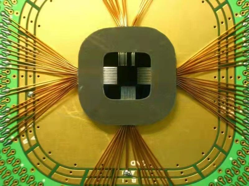
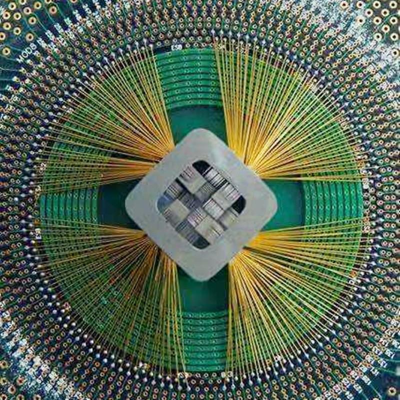
Substrate Compatibility: Supports wafer sizes from 2-inch (for specialty materials like GaN-on-SiC) to 12-inch (standard CMOS), with customizable pitch options (50μm to 500μm) to align with non-standard device layouts—critical for testing heterostructures or experimental device architectures.
Signal Integrity: Optimized for RF (up to 67GHz) and DC testing, with low parasitic capacitance (<0.2pF per channel) and crosstalk (<-80dB at 10GHz). Ideal for characterizing high-frequency devices or quantum dot structures requiring minimal signal distortion.
[Request Technical Datasheet →] | [Discuss Custom Configuration →]
Customization Capabilities: In-house design team can modify probe count (16 to 1024 channels), contact force (1g to 20g per probe), and thermal tolerance (-40°C to 150°C) to match specific research parameters—e.g., cryogenic testing of superconductors or high-temperature evaluation of wide-bandgap materials.
Comprehensive Customization Services
We understand that academic research often involves unique, non-standard testing scenarios, which is why our customization services are designed to adapt to your specific needs:
Full-Spectrum Design Adaptation: From initial concept to final production, we tailor every aspect of the probe card. Whether you need a probe card with an unconventional number of channels to match your custom device array, a specialized tip material to interact with a novel 2D semiconductor, or a modified substrate to withstand extreme testing environments (such as high vacuum or corrosive atmospheres), our engineers work with you to translate requirements into technical specifications.

[Request Technical Datasheet →] | [Discuss Custom Configuration →]
Rapid Prototyping & Iteration: For research projects in the early stages, we offer quick-turn prototyping of custom probe cards. This allows you to test and refine the design based on initial experimental results—whether adjusting probe spacing to align with newly fabricated pad layouts or modifying contact force to prevent damage to delicate nanostructures. Our typical prototyping cycle for small-batch custom designs is 2–3 weeks, ensuring minimal disruption to your research timeline.
Collaborative Specification Development: Our team doesn't just execute orders—we collaborate with you to define optimal customization parameters. For example, if you’re working on a project involving GaN power devices with non-uniform pad sizes, our engineers will analyze your device schematics and testing goals to recommend the ideal probe tip geometry, contact force range, and signal routing configuration, ensuring the probe card integrates seamlessly with your experimental setup.

[Request Technical Datasheet →] | [Discuss Custom Configuration →]
Research-Centric Support
Our engineering team includes PhDs in semiconductor device physics who collaborate with researchers to:
Validate probe card compatibility with novel substrates (e.g., flexible electronics, III-V heterostructures).
Optimize contact parameters via in-situ resistance monitoring during initial testing runs.
Provide detailed calibration reports (including probe planarity (<3μm across 300mm wafers) and signal delay matching (<5ps channel-to-channel)).
Case Example: Research Collaboration

Whether you're characterizing charge transport in 2D materials, prototyping power devices, or validating new lithography processes, our probe cards—backed by robust customization services—deliver the technical precision your research demands.
[Request Technical Datasheet →] | [Discuss Custom Configuration →]
Office Photo

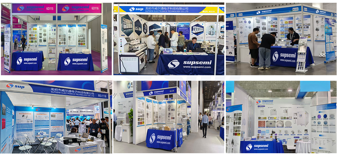
Exhibition
Contact: Bruce Liu
WhatsApp: +86-18059149998
Tel: +86-18059149998
Email: sales@supsemi.com
Add: Room 1402, Building 1, No. 89 Xibeilu, Xishancun, Xibei Street, Xinluo District, Longyan City, Fujian Province
We chat
