Welcome: Supsemi Electronic Technology Co., Ltd

sales@supsemi.com
+86-18059149998
Doping Type: N-type / P-type / Undoped
Crystal Orientation: 100 / 111 / 110 / 511
Crystal Process: Czochralski Single Crystal (CZ) / Float Zone Intrinsic (FZ)
Product Introduction:
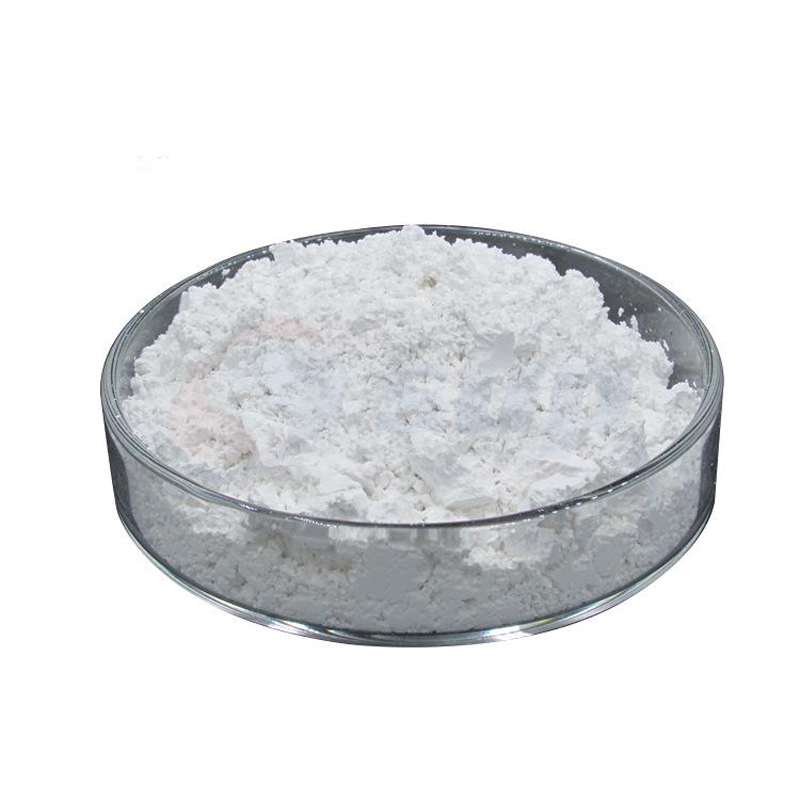
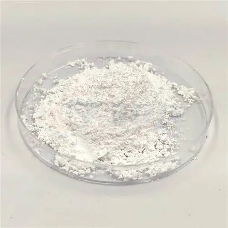
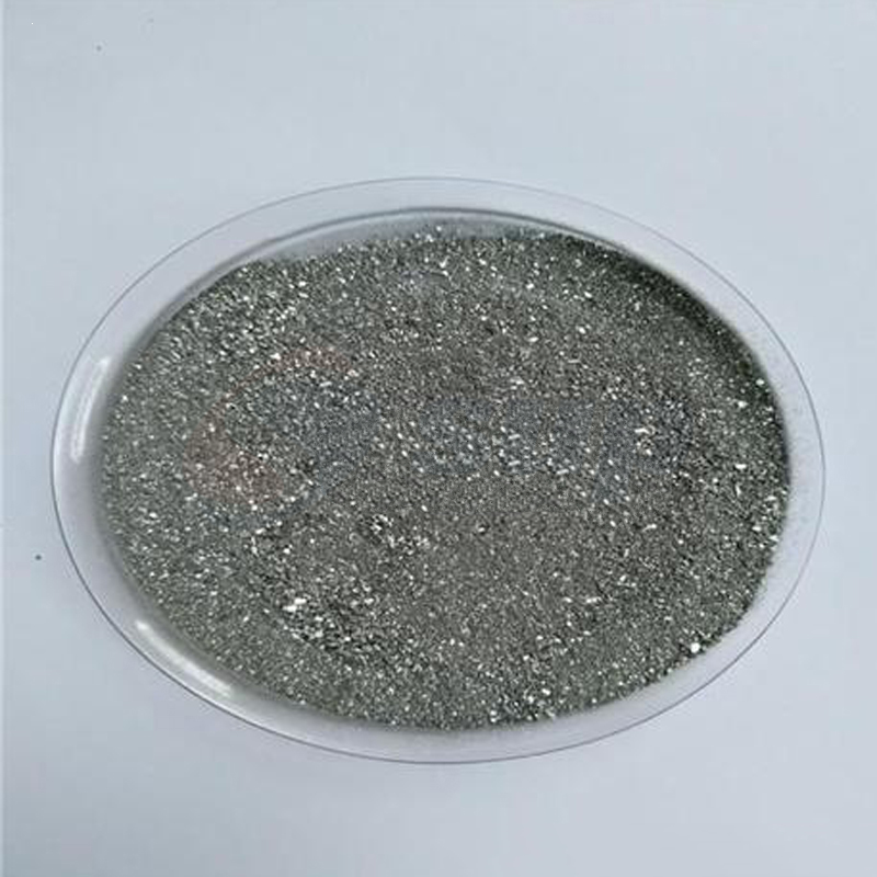
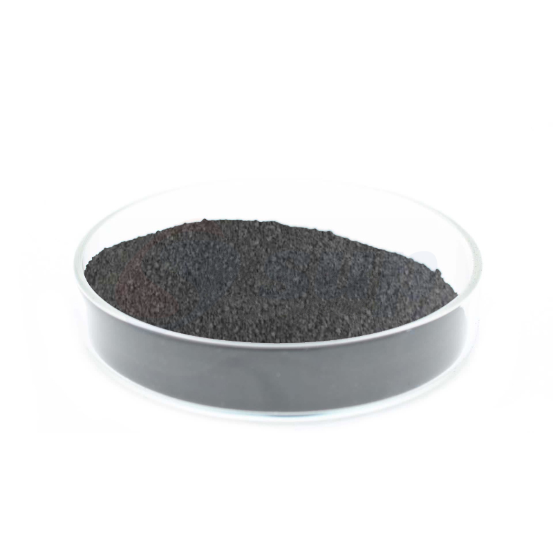
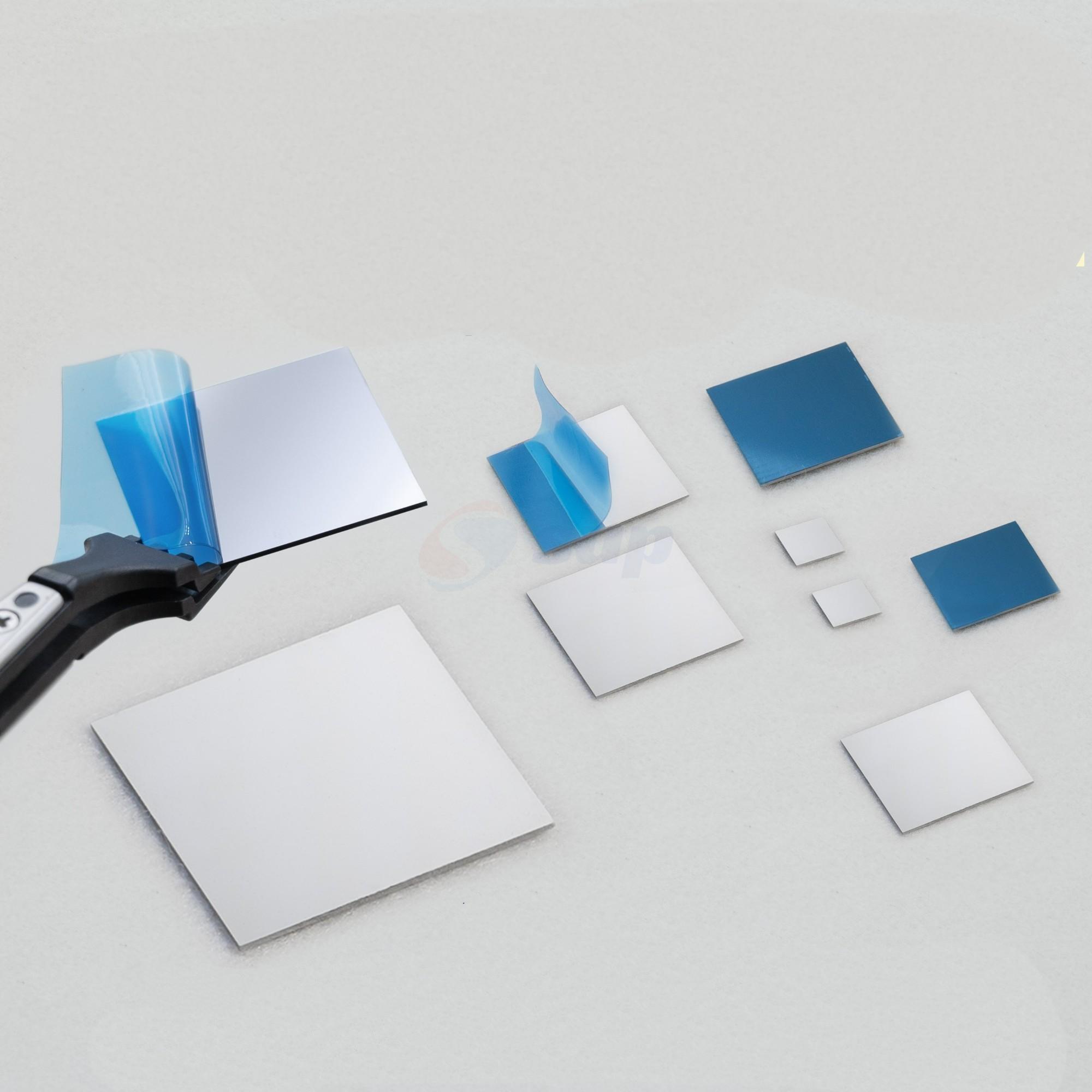
# Square Silicon Wafer Substrates: N-type & P-type, Customizable for Advanced Lab Applications
Square silicon wafers stand as foundational building blocks for cutting-edge laboratory analyses. Available in both N-type and P-type doping, these substrates are engineered to meet the stringent demands of techniques like SEM (Scanning Electron Microscopy), XPS (X-ray Photoelectron Spectroscopy), AFM (Atomic Force Microscopy), and PFM (Piezoelectric Force Microscopy).
[Request Quotation →] | [Discuss Custom Configuration →]
### Key Features:
- Doping Options: Choose between N-type (electron-dominant) or P-type (hole-dominant) wafers to align with your experimental needs, or opt for undoped substrates for baseline studies.
- Precision Customization: Tailored dimensions, thicknesses, and surface finishes (e.g., polished, etched) to fit SEM/XPS/AFM/PFM workflows—ideal for thin-film deposition, semiconductor device prototyping, or material characterization.
- High Purity & Uniformity: Fabricated via advanced Czochralski (CZ) or Float-Zone (FZ) processes, ensuring low defect density and consistent crystalline structure for reliable, reproducible lab results.
| Product Size | |||
| Retail reference price, if orders of more than 5 pieces, please contact us for a discounted wholesale price | |||
| Size | Price(USD) | Size | Price(USD) |
| 1 x 1 mm | 5 | 10 x 10 mm | 10 |
| 2 x 2 mm | 5 | 12 x 12 mm | 12 |
| 3 x 3 mm | 6 | 15 x 15 mm | 12 |
| 4 x 4 mm | 6 | 20 x 20 mm | 14 |
| 5 x 5 mm | 7 | 25 x 25 mm | 16 |
| 6 x 6 mm | 7 | 30 x 30 mm | 18 |
| 7 x 7 mm | 8 | 40 x 40 mm | 22 |
| 8 x 8 mm | 8 | 50 x 50 mm | 25 |
| 9 x 9 mm | 8.5 | ||
[Request Quotation →] | [Discuss Custom Configuration →]
### Applications:
Perfect for research in semiconductor physics, nanomaterial development, surface science, and device fabrication. Whether analyzing surface topography via AFM, probing chemical composition with XPS, or testing piezoelectric responses with PFM, these wafers deliver the stability and quality labs require.
Upgrade your experimental setup—explore customizable square silicon wafer substrates for SEM, XPS, AFM, and PFM today. Reach out to discuss your specs, and let’s advance your research together.


[Request Quotation →] | [Discuss Custom Configuration →]
Office Photo

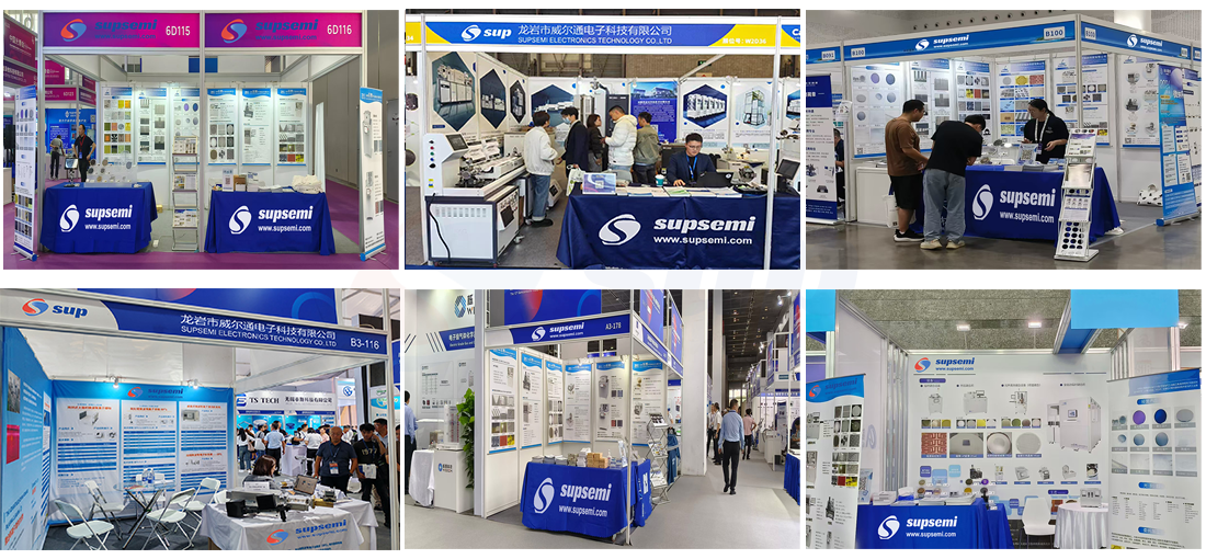
Exhibition

Contact: Bruce Liu
WhatsApp: +86-18059149998
Tel: +86-18059149998
Email: sales@supsemi.com
Add: Room 1402, Building 1, No. 89 Xibeilu, Xishancun, Xibei Street, Xinluo District, Longyan City, Fujian Province
We chat