Welcome: Supsemi Electronic Technology Co., Ltd

sales@supsemi.com
+86-18059149998
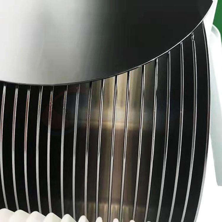
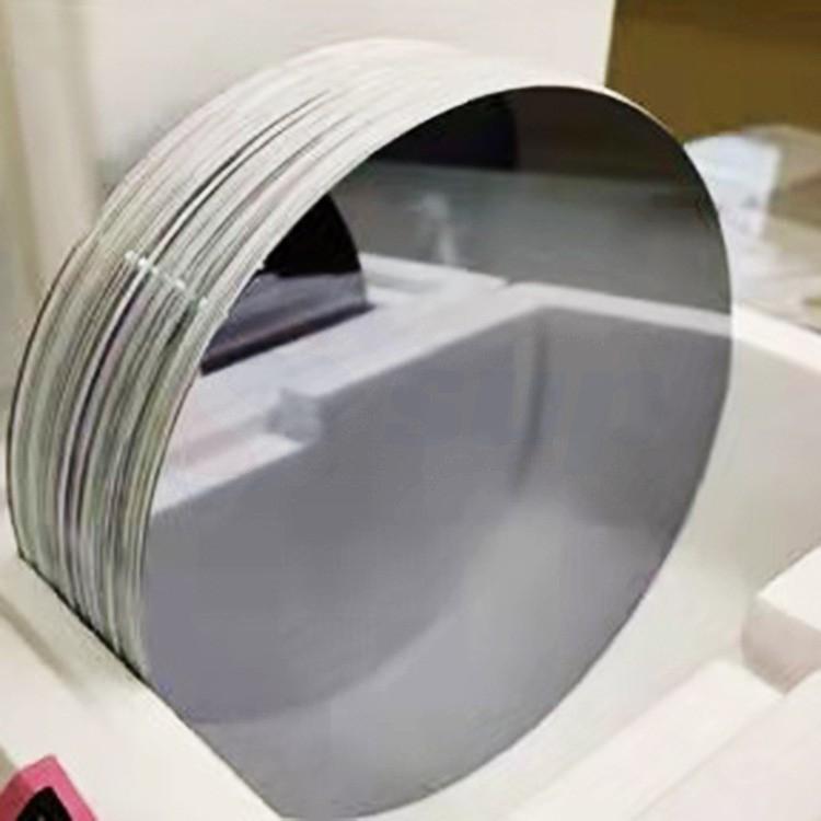
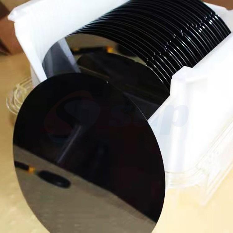
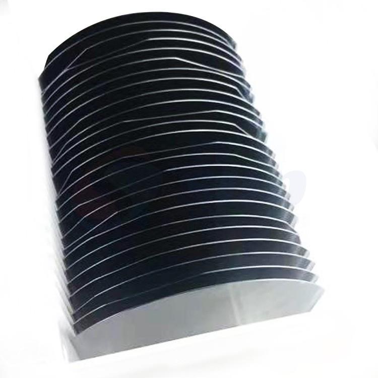
Our test wafers and dummy wafers are engineered for precision in semiconductor testing and equipment calibration.
We have 4 inch,6 inch,8 inch and 12 inch test wafers.
Trusted by manufacturers worldwide, our wafers streamline your workflow while reducing operational costs.
We offer 4-inch, 6-inch, 8-inch, and 12-inch test wafers, and support small-batch custom production. For details, please contact us to get the latest quotation! [Request Quotation →] | [Discuss Custom Configuration →]
Test Wafers: Precision Tools for Semiconductor Research
When your research hinges on accurate data and consistent performance, the right test wafers aren’t just components—they’re the backbone of reliable results. Our test wafers are engineered to meet the exacting needs of semiconductor researchers, with a focus on specificity, versatility, and traceability that sets them apart.
[Request Quotation →] | [Discuss Custom Configuration →]

Tailored to Your Research Focus
We offer a comprehensive range of test wafers designed for distinct research applications:
Material Characterization Wafers: Available in silicon, germanium, and compound semiconductors (GaAs, InP), these wafers come with pre-calibrated surface properties (roughness, oxide thickness) to simplify analysis of thin-film deposition, etching, or doping processes.
Metrology-Grade Wafers: Built with sub-micron dimensional accuracy (TTV < 50nm, Bow < 10μm), they’re ideal for validating measurement tools like ellipsometers, AFM systems, or wafer profilers—ensuring your equipment delivers precise readings before critical experiments.
Process Development Wafers: Customizable with predefined patterns (e.g., photolithography alignment marks, metal test structures) to streamline testing of new fabrication workflows, from lithography step optimization to thermal annealing studies.
[Request Quotation →] | [Discuss Custom Configuration →]

Why Researchers Trust Our Test Wafers?
Traceable Performance: Each wafer includes a detailed certificate of analysis (CoA) with batch-specific data—including resistivity (±0.01 Ω·cm), dopant concentration, and particle count (<10 particles >0.1μm)—so you can correlate results to material properties with confidence.
Consistency Across Batches: Our proprietary manufacturing process minimizes variability, ensuring that wafers from the same lot (or even different production runs) perform uniformly. This stability is critical for long-term research projects where repeatability is non-negotiable.
Cost-Effective Scalability: Whether you need 100mm wafers for lab-scale trials or 300mm options for pilot-line testing, we offer flexible quantities without compromising quality. Small-batch orders (as few as 5 units) are available for early-stage experiments, while bulk pricing supports large-scale research initiatives.
[Request Quotation →] | [Discuss Custom Configuration →]

Designed for Research-Critical Environments:
From cleanroom-based device fabrication to academic material science labs, our test wafers thrive in the conditions that matter most to your work:
Low-Contamination Surfaces: Cleaned to Class 10 standards (ISO 14644-1) and packaged in anti-static, hermetic containers to prevent particle adsorption during storage or transport—vital for experiments sensitive to surface impurities.
Compatibility with Advanced Tools: Optimized for use with leading semiconductor equipment (e.g., Applied Materials, TEL, ASML), these wafers ensure seamless integration with your existing workflow, reducing setup time and minimizing errors.
[Request Quotation →] | [Discuss Custom Configuration →]

Partner With a Team That Speaks Your Language
We understand that research timelines are tight and requirements are unique. Our technical support team includes former semiconductor researchers who can help you select the right wafer specs (e.g., crystal orientation, resistivity range) or even develop custom solutions—like wafers with patterned test structures tailored to your specific device architecture.
Every test wafer is backed by full traceability documentation, including raw material sourcing, manufacturing parameters, and quality control reports, so you can defend your data with confidence in peer reviews or patent applications.
Ready to elevate your research? Contact us today to discuss your project’s needs—we’ll help you find the test wafers that turn variables into valuable insights.
[Request Quotation →] | [Discuss Custom Configuration →]
Office Photo

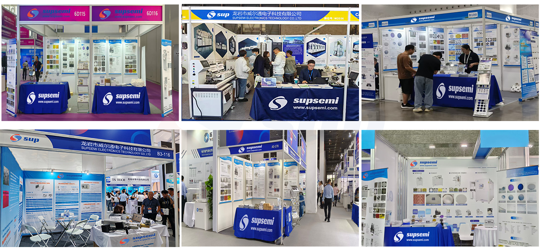
Exhibition
Contact: Bruce Liu
WhatsApp: +86-18059149998
Tel: +86-18059149998
Email: sales@supsemi.com
Add: Room 1402, Building 1, No. 89 Xibeilu, Xishancun, Xibei Street, Xinluo District, Longyan City, Fujian Province
We chat
